Falling Behind the Wind
Submitted by: Submitted by superman136
Views: 128
Words: 698
Pages: 3
Category: Literature
Date Submitted: 04/09/2014 08:55 PM
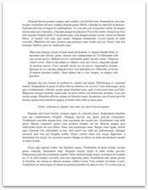
Arduino UNO Reference Design
TM
Reference Designs ARE PROVIDED "AS IS" AND "WITH ALL FAULTS". Arduino DISCLAIMS ALL OTHER WARRANTIES, EXPRESS OR IMPLIED, REGARDING PRODUCTS, INCLUDING BUT NOT LIMITED TO, ANY IMPLIED WARRANTIES OF MERCHANTABILITY OR FITNESS FOR A PARTICULAR PURPOSE Arduino may make changes to specifications and product descriptions at any time, without notice. The Customer must not rely on the absence or characteristics of any features or instructions marked "reserved" or "undefined." Arduino reserves these for future definition and shall have no responsibility whatsoever for conflicts or incompatibilities arising from future changes to them. The product information on the Web Site or Materials is subject to change without notice. Do not finalize a design with this information. VIN
RN1B 10K
3 5 6
IC1
IN OUT
+5V
4 2
7
2
+3V3
10K RN1A 8 1
2
8
1
CMP
3
U1A
1
U1B
7
MC33269ST-5.0T3 +5V +5V PC2 C2 47u 100n
LM358D GND GATE_CMD +5V +5V
LM358D
3
1 2
C1 100n
4
3
VIN D1 M7 PC1 47u
3
+
IC2 GND MC33269D-5.0
VI ADJ
1
VO
2
+
1
2
PWRIN
GND
GND
USBVCC
GND
1 IN EN GND NC/FB 4 OUT 5 +3V3
GND
GND
GND
GND
T1 FDN304V
3 2
C3 1u
+5V POWER
RESET
1 2 3 4 5 6
GND GND +5V ICSP1
1 3 5 2 4 6
+3V3
GND
+5V
4 5 6
VIN GND
RESET TS42
YELLOW L
RN4D 1K GND
1K RN2B
2
3
RN4C 1K
RN2A
10K RN1C 6 3
ICSP GND F1 X2
1 2 3 4
100n
500mA XUSB DD+
PGB1010604 Z2
DTR
USBVCC
GND
XT2 R1 RD- 1M RD+ Y1 XT1 16MHz +5V
RESET Y2 XTAL2 R2 1M XTAL1 AREF +5V
1
4
RESET2
24 2
22R RN3A 8 1 22R RN3D 5 4
PGB1010604
USB
P$2 P$1
XT1R
R3 27R
32 4 3
1
(PCINT7/OC0A/OC1C)PB7 (PCINT6)PB6 (PCINT5)PB5 RESET(PC1/DW) (T1/PCINT4)PB4 (PD0/MISO/PCINT3)PB3 (PDI/MOSI/PCINT2)PB2 XTAL2(PC0) (SCLK/PCINT1)PB1 (SS/PCINT0)PB0 XTAL1 AVCC VCC GND UCAP UVCC DD+ UGND PAD (INT4/ICP1/CLK0)PC7 (OC1A/PCINT8)PC6...