Ccs Timing and Noise Modeling in 45nm Designs
Submitted by: Submitted by bcang78
Views: 410
Words: 2873
Pages: 12
Category: Science and Technology
Date Submitted: 02/18/2013 06:35 AM
CCS Timing and Noise Modeling In 45nm Designs
Ang Boon Chong Sherine Ang Shor Lin Teoh Chea Ying
2
Agenda
• Introduction • CCS Timing
– Timing Modeling NLDM CCS – CCS vs NLDM Modeling Comparison Driver Comparison Scaling Receiver – CCS Timing Conclusion
• CCS Noise
– – – – CCSN Concept CCSN Generation Approach PT Hspice Correlation CCS Noise Conclusion
3
Introduction
VDD1
Less V&T Corners • Multi-Voltage Design • IR-Drop based STA
VDD2
Non-linear Waveforms: • High Impedance nets • Miller Effect • Signal Integrity • Double Switching
NLDM
1.20V, -40C 1.15V, -40C 1.10V, -40C 1.05V, -40C 1.00V, -40C 0.95V, -40C 0.90V, -40C
Voltage
1.20V, 25 C 1.15V, 25 C 1.10V, 25 C 1.05V, 25 C 1.00V, 25 C 0.95V, 25 C 0.90V, 25 C 0.85V, 25 C 0.80V, 25 C
1.20V, 125 C 1.15V, 125 C 1.10V, 125 C 1.05V, 125 C 1.00V, 125 C 0.95V, 125 C 0.90V, 125 C 0.85V, 125 C 0.80V, 125 C 0.80V, -40C 1.20V, -40C
CCS
1.20V, 125 C
Source: Synopsys Inc.
1.00V, -40C 1.00V, 125 C
0.80V, 125 C
Source: R. Chau, Intel 2003
0.85V, -40C 0.80V, -40C Temperature
Characterization: 6 Corners Accuracy: 2-3% vs. HSPICE
Characterization: 27 Corners
Source: Courtesy of Synopsys Inc.
Nonlinear Effects of Process Variation • Statistical models
4
CCS Timing-Timing Modeling
• Timing Modeling
– Primary focus is on the driver and receiver model
Figure 1 : Single Stage Calculation Model
5
Timing Modeling-NLDM Driver & Receiver
• Driver represent by Thevenin model
Vout Z net Vin Rd Z net
Figure 2 : Thevenin Model
• Receiver represent by simple load
6
Timing Modeling-CCS Driver & Receiver
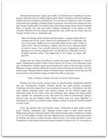
• Driver represent by current pulse
6.00E-02 5.00E-02 4.00E-02 3.00E-02 original selected 2.00E-02
•Selected point is modeled within CCS timing pulse LUT
1.00E-02
0.00E+00 1.4 -1.00E-02 1.5 1.6 1.7 1.8 1.9 2 2.1 2.2 2.3
Figure 3 : CCS Current Sample As Compare to Original Current Pulse
• Receiver model capture the change...
More like this
- Ccs Timing And Noise Modeling In 45Nm Designs
- Showbizltd.Com Announced 2014-2015 Contact Lists For Auditions, Jobs In Film, Television Production, Media, Print. Employment Connections Acting, Production, Models, Directing, Writers, Designers
- Building Design Predictions And Models
- Design And Control Of Warehousing
- An Overview Of Pricing Models For Revenue Management
- Model
- Robust Design
- System Analysis And Design
- Improving Design Capabilities For Automotive Industries In Malaysia
- Universal-Principles-Of-Design