Mobile Charger Circuit
Submitted by: Submitted by zeuben
Views: 403
Words: 575
Pages: 3
Category: Business and Industry
Date Submitted: 08/05/2012 06:35 AM
Mobile Cellphone Battery Charger Circuit
Charging of the mobile phone, cellphone battery is a big problem while traveling as power supply source is not generally accessible. If you keep your cellphone switched on continuously, its battery will go flat within five to six hours, making the cellphone useless.
A fully charged battery becomes necessary especially when your distance from the nearest relay station increases. Here’s a simple charger that replenishes the cellphone battery within two to three hours. Basically, the charger is a current-limited voltage source. Generally, cellphone battery packs require 3.6-6V DC and 180-200mA current for charging. These usually contain three NiCd cells, each having 1.2V rating.
Current of 100mA is sufficient for charging the cellphone battery at a slow rate. A 12V battery containing eight pen cells gives sufficient current (1.8A) to charge the battery connected across the output terminals. The circuit also monitors the voltage level of the battery. It automatically cuts off the charging process when its output terminal voltage increases above the predetermined voltage level.
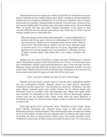
Circuit diagram:
Portable Cellphone Battery Charger Circuit Diagram
Parts:
P1 = 20K
P2 = 20K
R1 = 390R
R2 = 680R
R3 = 39R-1W
R4 = 27K
R5 = 47K
R6 = 3.3K
R7 = 100R-1W
C1 = 4.7uF-25V
C2 = 0.01uF
C3 = 0.001uF
D1 = 5.6V-1W Zener
D2 = 3mm. Red LED
Q1 = SL100
S1 = On/Off Switch
B1 = 1.5vx8 AA Cells in Series
IC1 = NE555 Timer IC
Circuit Operation:
Timer IC NE555 is used to charge and monitor the voltage level in the battery. Control voltage pin 5 of IC1 is provided with a reference voltage of 5.6V by zener diode D1. Threshold pin 6 is supplied with a voltage set by P1 and trigger pin 2 is supplied with a voltage set by P2. When the discharged cellphone battery is connected to the circuit, the voltage given to trigger pin 2 of IC1 is below 1/3Vcc and hence the flip-flop in the IC is switched on to take output pin 3...
More like this
- Mobile Charger Circuit
- Business
- Dell Cell Phone - Term Paper
- Solar
- Lte Air Interface Document
- Global And China Mobile Phone Charger Industry 2014 Market Trend, Size, Share, Growth Research Report
- Mobile Phones
- Mobile Banking
- Global System Of Mobile Communication
- Case Study Of Samsung's Mobile Phone Business